


Down-and-up: Combining DNA self-assembly with top-down fabrication
Jussi Toppari
Nanoscience Center & Department of Physics, P.O.Box 35, 40014 University of Jyväskylä, Finland
The molecular electronics as well as molecular scale optics, i.e. plasmonics, have long been visualized to pose the next big leap in technology development. The field is indeed developing rapidly thanks to the vast amount of research going on – but there is still a lot to do to fulfill the big promises. At a moment, DNA has proven to be a one of the most versatile and promising molecule for nanoscale fabrication [1]. Quickly developing techniques based on DNA self-assembly provide precise and programmable ways to form molecule scale devices for electrical and plasmonic purposes [2]. Since the self-assembly happens in a fully parallel manner, one can simultaneously fabricate huge amounts of devices. However, since the assembly happens in a solution, one needs a way to combine these bottom-up methods with some top-down method to – in the simplest case – position the assembled devices. Yet, combining the self- assembly directly with top-down methods during the fabrication, can yield even more versatile fabrication methods.
We have developed a method to trap and connect single molecular scale devices with other electrical circuitry, and utilized this to study the conductance of several types of individual DNA- nanostructures [2]. Since conductivity of DNA-helix seems to be too fragile to be utilized as such, we have realized a more robust realization of DNA-based electrical device, which utilized DNA nanostructures to assemble a row of gold nanoparticles (AuNP) [3]. The whole entity is further trapped between metallic electrodes where AuNPs act as metallic islands to form a single electron transistor (SET). Due to small size of the islands, this SET could work even at room temperature in contrast to the usually needed kryogenic temperatures. For nanoscale optics, we have developed a novel method, which takes advantage of the DNA origami constructions and together with conventional top-down nanofabrication processes enables fabrication of high quality sub-100-nanometer plasmonic nanostructures with desired shapes [4]. As a demonstration, we have fabricated optical bowtie antennas with a tunable plasmonic resonance in visible range. The method enables also fabrication of large optically chiral surfaces with high coverage. This ability to fabricate metallic nanoparticles with designed shape in high quantities provides great potential in various applications, especially sensing and metamaterial fabrication. Recently, we have further developed the method to enable its use with any substrate, and also to utilize other biomolecules [5]. To obtain the best possible optical response, we are developing a method to organize large lattices out of origami and fabricating metamaterials out of that. So far, this kind of lattices have been fabricated mainly on mica, which is not compatible with almost any topdown methods [6]. Thus, transporting the methods on silicon will open new avenues for DNA-based fabrication.
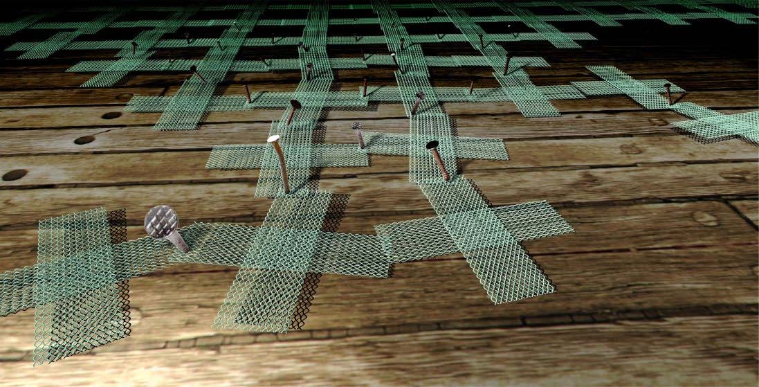
Fig. Fabricating DNA-origami lattices
References:
[1] A.V. Pinheiro, et al., Nat. Nanotech. 6, 763 (2011); M. Madsen, K.V. Gothelf, Chem. Rev. 119, 6384 (2019).
[2] V. Linko, J.J. Toppari, SAME 1, 101 (2013); L.N. Liu, T. Liedl, Chem. Rev. 118, 3032 (2018).
[3] K. Tapio, J. Leppiniemi, B. Shen, V.P. Hytönen, W. Fritzsche, J.J. Toppari, Nano Lett., 16, 6780 (2016).
[4] B. Shen, et al. Nanoscale, 7, 11267 (2015); B. Shen, et al. Science Adv. 4, eaap8978 (2018).
[5] P. Piskunen, B. Shen, A. Keller, J.J. Toppari, M.A. Kostiainen, V. Linko, ACS Appl. Nano Mat 4, 529 (2021).
[6] J.M. Parikka, K. Sokołowska, N. Markešević and J.J. Toppari, Molecules 26, 1502 (2021).
Acknowledgment: This work was supported by Academy of Finland, as well as Aatos and Erkko Foundation.

© 2026 · Biophotonics4Future
Leibniz Institute of Photonic Technology
Albert-Einstein-Str. 9
07745 Jena | Germany
www.leibniz-ipht.de