Skip to content

EACON 2020

EurAsian Conference on Nanophotonics

April 6 – 9, 2020 / Jena, Germany

Shih-Yen Lin

Research Center for Applied Sciences, Academia Sinica 11529, Taipei, TAIWAN
Graduate Institute of Electronics Engineering, National Taiwan University, TAIWAN

The Nature of van der Waals Epitaxy

Compared with traditional semiconductor materials, one of the major advantages of 2D materials is that their unique characteristics can be observed within several atomic layers, which makes them suitable for device applications in nm linewidths. Besides the search of new 2D materials, an alternate approach to enhance the device performances is through the stacking of different 2D materials. In this report, we will demonstrate the establishment of different2D material hetero-structures through the van der Waals epitaxy. MoS2/graphene hetero-structures is established through chemical vapor deposition for photo-transistor applications [1]. Vertical WS2/MoS2 hetero-structures is fabricated through sequential metal deposition/sulfurization procedures [2]. The atomic layer etching and the equivalent selective etching of the 2D material hetero-structures are also demonstrated [3]. On the other hand, the other group-V 2D material antimonene can also be grown on both WSe2 and MoS2 surfaces by using the van der epitaxy [4]. The much lower contact resistance of the conducting (elemental)/semiconductor (compound) 2D material interfaces will be advantageous for the practical application of 2D devices. The less dependence of the van der Waals epitaxy on the substrate may also benefit hetero-structure establishments with large lattice constant mismatch between the epi-layers and the substrates.

Figure 1. Different 2D material hetero-structures (MoS2/graphene, WS2/MoS2, left figure) and the
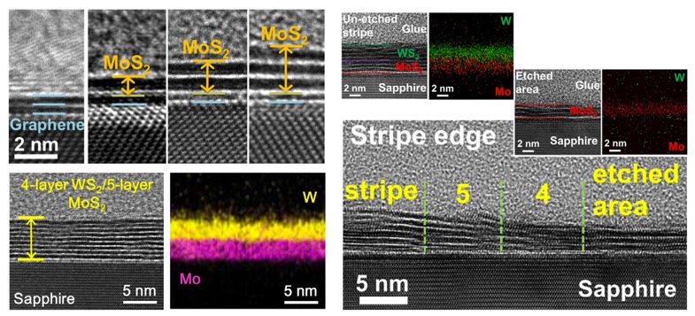
selective etching of the WS2/MoS2 hetero-structure (right figure).

References

  1. Meng-Yu Lin, Chung-En Chang, Cheng-Hung Wang, Chen-Fung Su, Chi Chen, Si-Chen Lee, and Shih-Yen
    Lin, Appl. Phys. Lett. 105, 073501 (2014).
  2. Chong-Rong Wu, Xiang-Rui Chang, Tung-Wei Chu, Hsuan-An Chen, Chao-Hsin Wu, and Shih-Yen Lin 16,
    7093 (2016).
  3. Kuan-Chao Chen, Tung-Wei Chu, Chong-Rong Wu, Si-Chen Lee and Shih-Yen Lin, 2D Materials 4, 034001
    (2017).
  4. Hsuan-An Chen, Hsu Sun, Chong-Rong Wu, Yu-Xuan Wang, Po-Hsiang Lee, Chun-Wei Pao, and Shih-Yen
    Lin, ACS Appl. Mater. Interfaces 10, 15058 (2018).

Further Talks

Andrea Csáki

Microfludic Synthesis of plasmonic Nanoparticles for Sensing Applications

Andrey Turchanin

Controlled growth of transition metal dichalcogenide monolayers for applications in nanoelectronic and nanophotonic devices

Chi Chen

Near Field Spectroscopic Imaging: from Hard to Soft Materials

Chi-How Peng

Cobalt mediated controlled/living radical polymerization: from mechanism understanding to materials application

Chun-Hong Kuo

Bridging Energy and Chemistry via Nanoarchitectonic Engineering at Atomic Scale

Falk Eilenberger

Integration of two-dimensional materials in optical systems for nonlinear optics, sensing, and single photon sources

Frank Setzpfandt

Nonlinear frequency conversion in nanostructured optical systems for application in quantum photonics

Heng-Liang Wu

Controlling the Oxidation State of Cu Electrode and Reaction Intermediates for Electrochemical CO2 Reduction to Ethylene

Kien-Voon Kong

Direct Observation of Reaction Intermediates of Metal-based Therapeutic Agents in Single Living Cell Using TERS

Maria Wächtler

Quantum confined semiconductor nanostructures in light-driven catalysis

Martin Presselt

Supramolecular Control of Optical and Electronical Properties of Two-Dimensional Dye Layers

Po-Chiao Lin

New Environment Sensitive Fluorophores with Color-Tailored Emission: In Vivo Monitoring of Carbonic Anhydrases Expression on Growth of Larval Zebrafish

Shangjr (Felix) Gwo

Plasmonic Metasurface-Enhanced Linear and Nonlinear Processes in Two-Dimensional Semiconductors

Ta-Jen Yen

Empowering Bilayer MoS2 by Engineered Plasmonic Nanostructures for Optoelectronic Applications

Tiow-Gan Ong

Carbodicarbene, Carbogenic Maverick, Not a Moderate!

Volker Deckert

Plasmon Enhanced Probe Spectroscopies – Structural Investigation of Nanoscale Objects

Yi-Tsu Chan

Molecular self-assembly methodology for rational construction of metallosupramolecules with high structural complexity

Yian Tai

Toward a universal polymeric material for electrode buffer layers in organic optoelectronics

Yu-Chieh Cheng

Kirigami-based soft robots with light-responsive properties

Yu-Jung Lu

Controlling Light-matter Interactions at Nanoscale with Plasmonics: From Spontaneous Emission to Lasing